Tata Electronics announced seven strategic MoUs with global technology leaders, domestic research bodies and infrastructure partners
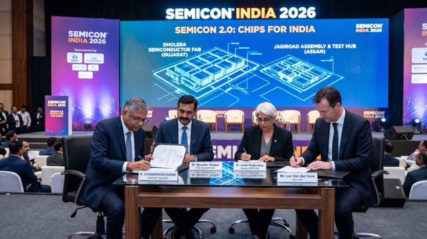
Semicon India 2026, Tata Electronics announced seven strategic Memorandums of Understanding (MoUs) with global technology leaders, domestic research bodies, and infrastructure partners. The agreements aim to build a robust, self-sustaining semiconductor ecosystem around Tata’s manufacturing hubs in Dholera, Gujarat (an $11 billion wafer fab) and Jagiroad, Assam (an advanced packaging facility), supporting the Government of India’s “Semicon 2.0” mission.
The 7 Strategic MoUs Breakdown
Nexperia (Netherlands) — Wafer Fab & Packaging Collaboration
- Dholera Fab (Gujarat): Front-end manufacturing of Nexperia’s MOSFET portfolio at Tata’s 300mm wafer fab.
- Jagiroad Facility (Assam): Back-end assembly and testing for Nexperia’s discrete semiconductor products.
BESI (Netherlands) — Advanced Packaging Capabilities
- Leverages BESI’s advanced packaging equipment and technology at the Jagiroad facility to serve high-growth sectors such as AI, high-performance computing, data centers, automotive, and consumer electronics.
Semi-Conductor Laboratory (SCL) — Design, Process Node & Skilling
- A government-private partnership with MeitY’s SCL focusing on chip design services for government/startups, technology node enablement, domestic
supply-chain localization, and workforce skilling.
Fujifilm Corporation (Japan) — Critical Materials & Local Manufacturing
- Focuses on the supply and development of advanced semiconductor materials for the Dholera fab.
- Fujifilm plans to invest approximately ₹800 crore ($83 million) to set up a phased semiconductor materials manufacturing plant in the Dholera Special Investment Region (DSIR).
JSR Corporation (Japan) — Photoresists & Advanced Chemicals
Secures a reliable supply chain of photoresists and high-purity process chemicals essential for advanced node manufacturing and yield stability at the Dholera fab.
Ascendas First Space — 363 Acre Supplier Vendor Park
- Development of a dedicated 363-acre vendor park in Dholera to host suppliers of equipment, raw materials, and specialized services. This cluster model aims to shorten lead times, mirroring semiconductor ecosystems in Taiwan and South Korea.
Gati Shakti Vishwavidyalaya (GSV) — Specialized Talent Pipeline
- Collaboration with GSV, L&T EduTech, and Jacobs Solutions to create tailored curricula, joint certifications, and workforce training focused on fab engineering, infrastructure systems, and logistics execution.
Key Takeaways & Strategic Impact
- Full-Stack Ecosystem Creation: The partnerships cover every stage of the semiconductor value chain—from design and raw materials to wafer fabrication, advanced packaging, vendor infrastructure, and skilled engineering talent.
- Total Investment Commitment: Tata Electronics has committed a total of $14 billion across its Dholera ($11 billion) and Jagiroad projects.
- Long-Term Operational Commitment: According to Tata Electronics CEO Dr. Randhir Thakur, these MoUs reflect operational commitments to lay the operational foundation, with financial value following as manufacturing ramps up.